X-RAY NDT
Introduction to NDT
Non destructive testing refers to the method of inspecting and testing the structure, nature, state, type, quantity, shape, position and size of the internal and surface of the test piece by taking advantage of the changes in thermal, acoustic, optical, electrical, magnetic and other reactions caused by the abnormal internal structure of the material or the existence of defects, on the premise of not damaging the service performance of the tested object and the internal organization of the tested object.
Significance of NDT
Without damaging the tested object, the above changes can be measured to help enterprises more comprehensively, directly and deeply understand and evaluate the nature, status, quality or internal structure of the tested materials and equipment components, which is conducive to monitoring product quality and improving process.
application area
PCB&PCBA, FPC, electronic appliances, electronic components, plastic materials, automotive materials and parts, medical equipment, institutions/research products, military industry and national defense, etc.
NDT means
1. CT detection
Rebuild the complete 3D model of the part from the inside out without destroying the part; Material defect analysis, failure form analysis, geometric and geometric tolerance measurement and assembly correctness.
Scope of application: electronic components, high-precision components, PCB/PCBA, etc.
Industrial CT inspection application projects: defect analysis, dimension measurement, CAD digital analog comparison
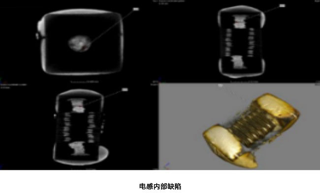
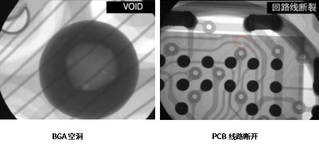
2.X-Ray Testing For the position where the sample cannot be detected by appearance, record the change of light intensity after X-Ray penetrates materials of different densities, and the contrast effect can be used to form an image to show the internal structure of the object to be tested, so that the problem area inside the object to be tested can be observed without damaging the object to be tested.
Scope of application: defect detection of internal cracks and foreign matters of metal materials and parts, plastic materials and parts, electronic components, electronic components, LED components, etc., and analysis of internal displacement of BGA, PCB, etc; Discriminate BGA welding defects such as empty welding and faulty welding, analyze the internal conditions of microelectronic systems and sealing elements, cables, fittings, plastic parts, etc.
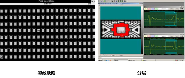
3.Ultrasonic scanning (C-SAM) NDT for delamination, crack and other defects (crack, delamination, cavity, etc.) of electronic components, LED and metal substrate; The difference of acoustic impedance inside the material is judged by image contrast, the shape and size of defects are determined, and the direction of defects is determined.
Scope of application: plastic packaging IC, chip, PCB, LED, etc.
Sample requirements CT: The sample size is generally required to be no more than 50mm x 50mm.
X-Ray: no more than 300mm x 300mm
C-SAM: No special requirements
Please call for special structure products, and the technical engineers will answer one-to-one!
|