Introduction to Morphology Observation and Measurement
The micro geometric shape of the surface is called surface topography. In recent years, with the development and progress of science and technology, higher and higher requirements have been put forward for the surface accuracy of various materials; At the same time, as users requirements for products are getting higher and higher, industry standards are getting stricter and stricter, and the automation level of manufacturing industry is improving, many industries are facing the reform of the entire process flow, so surface inspection is increasingly valued by enterprises.
Morphological observation and measurement significance
① The micro geometric morphology of the material surface has a great influence on its many technical properties and application functions.
② The observation of the surface morphology of the material provides convenience for the study of the morphology and structure of the sample, helps to monitor the product quality and improve the process.
application area
Materials, electronics, lead-free welding, machining, semiconductor manufacturing, aviation, automobile, ceramics, geology, medicine, metallurgy, etc.
Test process
Sample requirements
Sample requirements for electron microscope observation: non-magnetic or weakly magnetic, solid sample that is not easy to deliquescence and is not volatile, less than 8CM * 8CM * 2CM.
Sample requirements for optical microscope observation: no special requirements.
testing procedure
Confirm sample type → confirm inspection specification → observe sample → record observation phenomenon/measure data evaluation → result evaluation
Reference Standards
1. CSIC Testing Laboratory recommends standards according to sample conditions
2. Standards provided or suggested by customers
Common standards (partial)
JYT 010-1996 General rules for analytical scanning electron microscopy
GB/T 16594-2008 General Rules for Measuring Micron Length by Scanning Electron Microscope
IPC-6012 Qualification and Performance Specification for Rigid Printed Boards
IPC-A-610 Acceptability of electronic components
JIS B 0601-2013 Geometrical Product Specifications (GPS) - Surface texture profile method - Terms, definitions and surface texture parameters
We invite you to share the selected cases of CSI Testing Laboratory over the years and the pure dry goods technical knowledge!
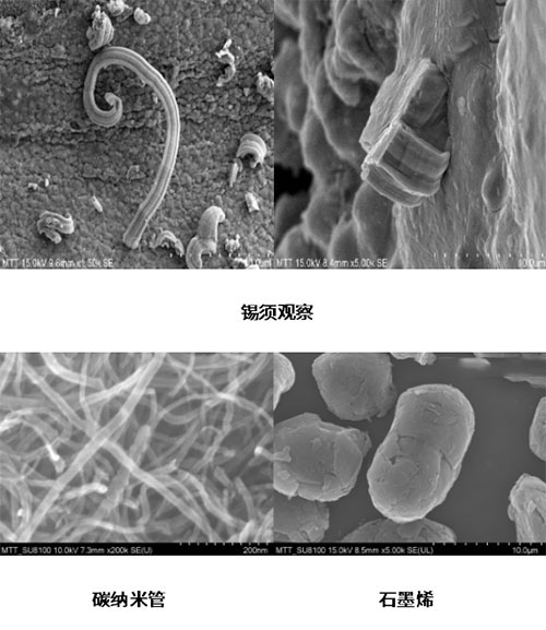
1. Observation and measurement of surface morphology
The main content of scanning electron microscope is to analyze the geometric morphology, particle size and particle size distribution of materials, phase structure, etc.
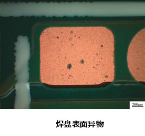
The optical microscope is mainly used for the verification of tooling inspection tools and metal parts, the inspection of electronic product assembly, offset and welding anomalies, the inspection of PCB/PCBA lines, anti welding, holes, part alignment and text and graphic defects.
2. Characteristic size measurement

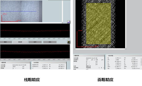
3. Surface roughness analysis